STAR-Tiger is a high-performance SpaceFibre routing switch. A power supply board in the STAR-Tiger unit provides the primary power rails to the Xilinx KU060 FPGA being used to implement the routing switch. The STAR-Tiger power supply design is shown in Figure 1, along with a photograph of the board in Figure 2. The STAR-Tiger power supply board uses radiation hard power supply devices from Texas Instruments. A white paper describing the power supply design is available at “STAR-Tiger Power Supply Paper” and links to the components used are provided at “STAR-Tiger” on the Texas Instruments website.
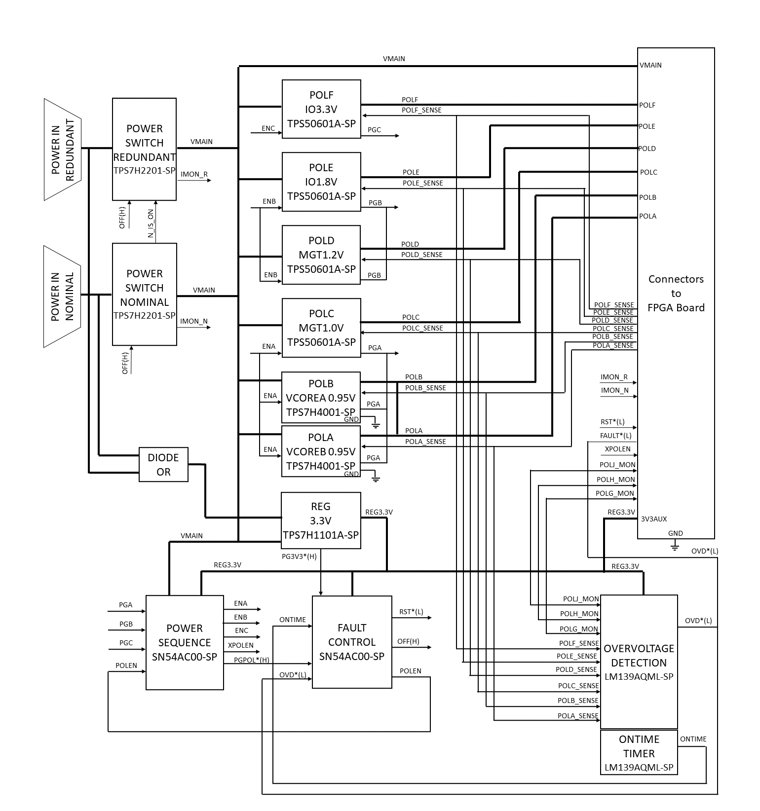
Figure 1: STAR-Tiger Power Supply Board Block Diagram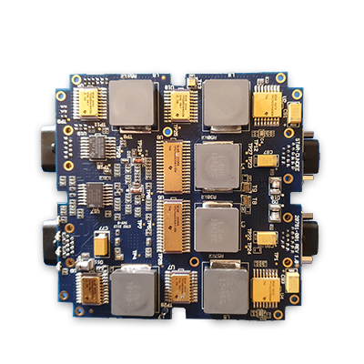 Figure 2: STAR-Tiger Power Supply Board
There are two power inputs to the power supply board, PWR-N and PWR-R (nominal and redundant). The power input is nominally 5V ±5% at up to 12A. Each power input goes to a power switch (TPS7H2201-SP) which is used to switch power from either the nominal or the redundant power input to an array of point-of-load (POL) converters. The power switches are controlled by a fault detection circuit using the OFF(H) signal which, when asserted, switches off the power switches. During normal operation only one power switch is provided with power.
When power is applied to the nominal power input, the nominal power switch is turned on and the redundant one turned off.
When power is applied to only the redundant power input, the nominal power switch is turned off and the redundant one turned on.
When power is applied to both nominal and redundant power inputs, the nominal power switch is turned on and the redundant one turned off, so that power is drawn from the nominal power input only.
The power switches protect the SpaceFibre routing switch from overvoltage (up to 7V) and reverse polarity. The switched 5V rail provides the main supply voltage (Vmain) to several POL DC-DC converters and to a regulator. Each of these devices can operate with a power input of up to 7V. The power switches provide overvoltage protection which will switch off the Vmain power should the input voltage exceed the maximum power input voltage.
The power switches have overcurrent and overtemperature protection and also a current sense output. The overcurrent limit is set to 17.6A maximum, which takes into account the normal maximum current, current inrush during power up and 20% tolerance on the overcurrent limit setting. Power will be switched off when the overcurrent condition has been present for around 1ms. There are two current sense outputs, IMON, one on each power switch device.
Vmain from the power switches is used to drive the POL converters which provide the POLA, POLB, POLC, POLD, POLE and POLF output voltage for the FPGA. For a Xilinx KU060 FPGA these correspond to VCOREA0.95V, VCOREB0.95V, MGT1.0V, MGT1.2V, IO1.8V and IO3.3V power rails respectively. A pair of TPS7H4001-SP regulators provide the POLA/POLB supplies, and four TPS50601A-SP regulators are used for POLC, POLD, POLE and POLF. The output from each POL converter is passed to the connector on the power supply board, which is used to provide power to the FPGA and other boards. VCOREA0.95V and VCOREB0.95V are connected together for the Xilinx KU060 FPGA used in STAR-Tiger.
A voltage sense signal is also provided for each POL converter on another connector. Each sense signal is connected close to the load on the FPGA board and senses the voltage at the load, so that each POL can adjust the voltage to the required level.
Each POL converter has an output undervoltage and overvoltage detection circuit which checks that the output voltage is within 94-106% (typical), 97-103% (maximum) of its nominal value. If this voltage goes outside 91-109% (typical), 90-110% (maximum) of its nominal value the power good (PG) pin of that device will be de-asserted pulling the corresponding PGx signal low which will propagate through chain of POL converters causing PGPOL*(H) to be de-asserted. Note that the overvoltage switch-off threshold of the POL converters is not accurate enough to protect a Xilinx KU060 FPGA from overvoltage, so a separate overvoltage detection circuit is used.
Each POL converter is enabled by an EN input and indicates when its output has reached, or is close to, its required output voltage by asserting an open-drain power good signal. The POL converters are grouped into three groups:
- POLA, POLB and POLC (KU060 VCOREA0.95V, VCOREB0.95V and MGT1.0V, respectively)
- POLD and POLE (KU060 MGT1.2V and IO1.8V, respectively)
- POLF (KU060 IO3.3V)
POLs in a group are enabled by the same enable signal and generate PG only when all the POLs in the group have reached close to their nominal output voltage. The groups are arranged as follows:
- Group A enabled by ENA, generating PGA: POLA, POLB and POLC
- Group B enabled by ENB, generating PGB: POLD, POLE
- Group C enabled by ENC, generating PGC: POLF
A power sequencing circuit is used to determine the order of powering each group. For the KU060 FPGA the following sequence is followed
- Group A, POLA, POLB and POLC (VCORE0.95Vand MGT1.0V), enabled when Vmain > a threshold voltage
- Group B, POLD and POLE (MGT1.2V and IO1.8V), enabled when PGA is asserted, i.e. POLA, POLB and POLC have all reached close to their nominal voltage
- Group C, POLF(IO3.3V), enabled when PGB is asserted, i.e. POLD and POLE have both reached close to their nominal voltage
- A PGPOL*(H) signal is asserted by the power sequencing circuit when PGC is asserted, i.e. when all the POL converters have reached and remain at close to their nominal voltages, the PGPOL*(H) signal is asserted.
To ensure that all the POL converters are switched off in the event of one of them failing, it is necessary to disable those upstream on the EN chain. This is done using a fault control circuit.
The overvoltage detection in the POL converters is not accurate enough to be used for overvoltage protection of the FPGA, so a separate overvoltage detection circuit is used. This comprises a voltage reference (LM4050QML-SP) and set of comparators (LM139AQML-SP), one for each POL converter, which compares the sensed voltage against its maximum permitted value. If an overvoltage is detected, the overvoltage detection circuit asserts the OVD*(L) signal. In addition, there are three additional overvoltage detection circuits on the power supply board that can be used to monitor voltages on other boards in the STAR-Tiger unit and switch off the unit if a potentially damaging fault occurs. Additional POL converters on other boards are monitored by overvoltage circuitry on those boards. If an overvoltage is detected, a FAULT*(L) signal is asserted which drives the OVD*(L) signal on the power supply board, disabling power.
An additional POL enable signal, XPOLEN, is provided for the eXternal POL converters on the other boards in the STAR-Tiger unit. When XPOLEN is asserted the external POL converters are enabled.
The fault control circuit comprises a reset timer, ONTIME, (LM139AQML-SP) and some logic gates (SN54AC00) which are powered by a 3.3V regulator, REG_3V3, (TPS7H1101A-SP) that is powered by Vmain. When the input power switch turns on, the timer is powered by the regulator and its output remains asserted for a power-on timeout period. This power-on timeout is set to be longer than the maximum expected time for the POL converters to all power up and for PGC to be asserted. No faults can be detected during this initial power up interval. The power-on timeout is also used to provide a system reset signal. The following faults can be detected:
- The POL converters have not reached their power good state in the expected time period. This condition is detected by PGPOL*(H) not being asserted before the power-on timeout timer expires. The POL converters on the other boards are linear regulators and do not have power good outputs.
- One or more POL converters becoming overvoltage, undervoltage or overtemperature. This condition is detected by the POL converter with the fault de-asserting its power good signal which propagates along the POL power-good/enable chain resulting in PGPOL*(H) being de-asserted. The fault is detected when PGPOL*(H) is de-asserted at any time after the power-on timer has expired.
- The overvoltage detection circuit detects that one of the sensed voltages has exceeded a set threshold value and is in danger of damaging the FPGA. When this condition is detected on any of the sensed voltages, the OVD*(L) signal is asserted.
- The linear regulators on the FPGA board (POLG, POLH and POLJ) are also monitored by the overvoltage detection circuit on the power supply board.
- Other linear regulators on other boards are monitored by local overvoltage comparators. When an overvoltage fault is detected the FAULT*(L) signal is brought low. FAULT*(L) on the FPGA and other boards is connected to OVD*(L) on the PSU board, so when it is brough low, the power switches are turned off and the POL converters disabled.
- Overtemperature of the FPGA or the FPGA board. This condition is detected by a TMP461-SP temperature sensor on the FPGA board which monitors local (board) or remote (FPGA) temperature and which asserts the FAULT*(L) output when an overtemperature condition occurs.
When a fault occurs, the fault control circuit disables the POL converters and asserts the OFF(H) signal, switching off the two power switches. The fault control circuit and comparators are powered from the 3.3V regulator (REG_3V3), which is powered directly from the 5V nominal or redundant inputs. Diode ORing is used to combine these two power sources together for the REG_3V3 supply because the load is low. Since the fault control circuitry is not switched off by the power switches, the power switches remain disabled once a fault has occurred. To recover from this fault condition, it is necessary to power down both the nominal and redundant 5V inputs and to then turn one of them on again.
The REG_3V3 supply also provides the 3V3AUX supply to other boards which is used to power the overvoltage detection circuits on those boards.