Low Voltage Differential Signalling (LVDS) as defined in ANSI/TIA/EIA-644 is specified as the signalling technique for SpaceWire. LVDS uses balanced signals to provide very high-speed interconnection using a low voltage swing (350 mV typical). The balanced or differential signalling provides adequate noise margin to enable the use of low voltages in practical systems. The low voltage swing results in relatively low power consumption at high speed. LVDS is appropriate for connections between chips on a board, boards in a unit, and unit to unit interconnections over distances of 10 m or more. The LVDS signalling levels are illustrated in Figure 27.
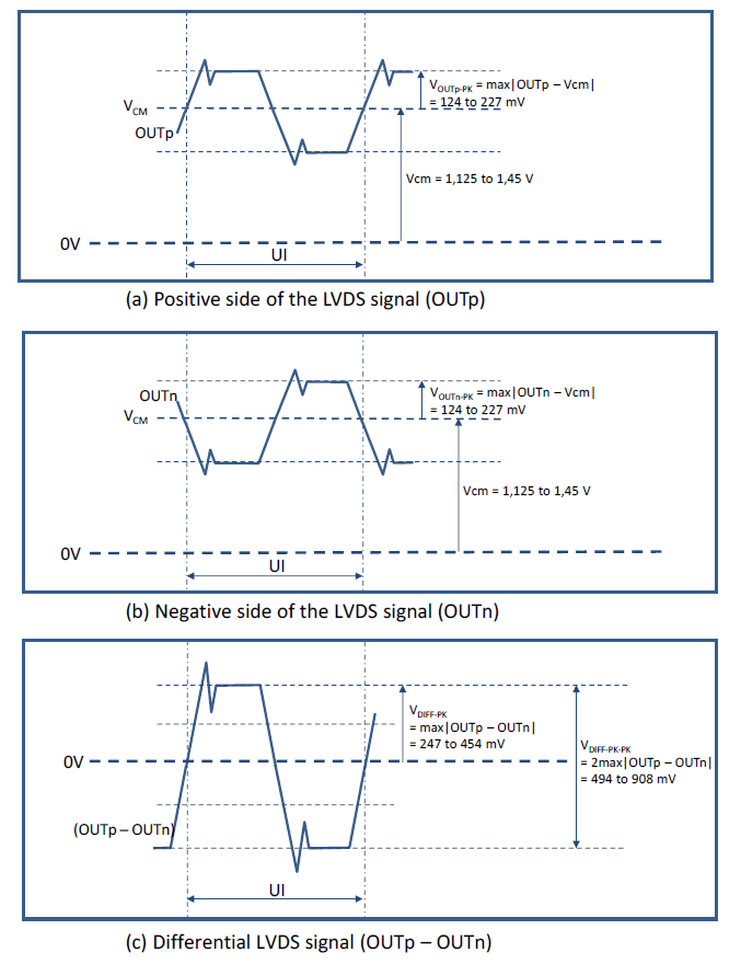
Figure 27 LVDS Signalling Levels
A typical LVDS driver and receiver are shown in Figure 28, connected by a media (cable or PCB traces) of 100 ohm differential impedance. The LVDS driver uses current mode logic. A constant current source of around 3.5 mA provides the current that flows out of the driver, along the transmission medium, through the 100 ohm termination resistance and back to the driver via the transmission medium. Two pairs of transistor switches in the driver control the direction of the current flow through the termination resistor. When the driver transistors marked “+” in Figure 28 are turned on and those marked “-” are turned off, current flows as indicated by the arrows on the diagram creating a positive voltage across the termination resistor. When the two driver transistors, marked “-”, are turned on and those marked “+” are turned off, current flows in the opposite direction producing a negative voltage across the termination resistor. LVDS receivers are specified to have high input impedance so that most of the current flows through the termination resistor to generate around ±350 mV with the nominal 3.5 mA current source.
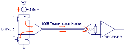
Figure 28 LVDS Operation
LVDS has several features that make it very attractive for data signalling:
- Near constant total drive current (+3.5 mA for logic 1 and -3.5 mA for logic 0) which decreases switching noise on power supplies.
- High immunity to ground potential difference between driver and receiver, LVDS can tolerate at least ±1 V ground difference.
- High immunity to induced noise because of differential signalling, normally using twisted-pair cable.
- Low EM emission because small equal and opposite currents create small electromagnetic fields which tend to cancel one another out.
- Not dependent upon particular device supply voltage(s).
- Simple 100 ohm termination at receiver.
- Failsafe operation – the receiver output goes to the high state (inactive) whenever
- the receiver is powered and the driver is not powered,
- the inputs short together,
- input wires are disconnected.
- Power consumption is typically 50 mW per driver/receiver pair for LVDS compared to 120 mW for ECL/PECL.
The signal levels and noise margins for SpaceWire are derived from ANSI/TIA/EIA-644 which defines the driver output characteristics and the receiver input characteristics. The eye diagram for SpaceWire signals sent over 10 m of cable at 200 Mbits/s baud rate is shown in Figure 29.
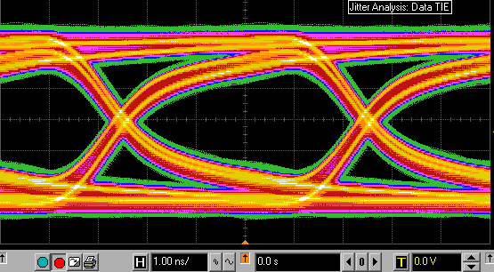
Figure 29 SpaceWire Eye Diagram (200MHz, 10 m cable)